
Don't Move The Data!
A prescient 2017-era article, with 2025 commentary.

Editor’s Note: This article was first posted on October 6, 2017 on the CUDA Handbook blog. It has been updated (with editor’s notes) to reflect developments between then and mid-2025.
NVIDIA just delivered their first Volta-enabled DGX-1 systems – great news for those who need additional compute power: each V100 chip delivers 15.7 TFLOPS of single precision performance, compared to its predecessor that only had 10.6 TFLOPS.
Wait, you say, that’s an interesting qualifier. Who doesn’t “need the additional compute power…?” Did someone hack into Nick’s blog account and post on his behalf? Or has he become a Luddite in his dotage?
Nope, no, I still think more compute is generally better; but it is past time to question the architecture of these systems with huge, discrete GPUs connected to the world by buses. The problem with DGX-1 is that those GPUs are hungry! They need to be fed! And they can only sip data through the tiny soda straw known as the PCI Express bus. (For a 2025 perspective, consider that NVIDIA claims 8,000GB/s per GB200 chip, compared to PCIe 6.0’s 128GB/s unidirectional bandwidth, for a 60x disparity between HBM bandwidth and bus bandwidth. Both of these numbers can be doubled: the Blackwell number because it is a two-die configuration, and the PCIe number because it supports 256GB/s bidirectional bandwidth. —Ed.)
For perspective, let’s compare these chips to G80, the first CUDA-capable GPU. Let’s set the stage by observing that G80 was the largest ASIC NVIDIA could feasibly design and fabricate in 2006, straining the limits of contemporary fabrication technology – a classic “win” chip. It had 684M transistors, a theoretical maximum performance of 384GFLOPS for single precision, and no support at all for double precision. GP100 and GV100 respectively have 22x and 31x more transistors, and 27x and 39x more single precision performance than G80. (In 2025, a Blackwell chip contains 104B transistors, 5x more than 2017’s V100, and they utilize packaging to effectively double that count. So each of the two chiplets has >150x as many transistors as the original CUDA-capable chip! —Ed.) But the bandwidth to deliver data to and from these GPUs has not been increasing commensurately with that performance.
                Transistors   SPFOPS   Bandwidth
Chip  Date       (billions)  (TFLOPS)    (G/s)    FLOPS/byte
 G80  11/8/2006      0.7        0.38       86.4      4.4
GT200 6/16/2008      1.4        0.93      141        6.6
GF100 3/26/2010      3.1        1.35      177        7.6
GK110 11/12/2012     7.0        4.3       288       14.9
P100  4/5/2016      15.3       10.6       732       14.5
V100  6/21/2017     21.2       15.7       900       17.4
A100  5/14/2020     54.2       19.5      2000        9.8
H100  3/22/2022     80         67        3350       20.0
H200  11/28/2024    80         67        4800       14.0
B200  1/30/2025    104         80        8000       10.0
There is an inflection point in the chart with the introduction of HBM (P100, c. 2016), the memory technology invented to keep GPUs from starving. HBM was able to keep the FLOPS/byte from continuing to diverge at the same rate.
Several other important developments are not reflected in this table:
TensorCores, which greatly increase the theoretical FLOPS counts deliverable by chips since V100 (c. 2017),
NVIDIA has pivoted their product designs (and marketing) to focus on peak FLOPS numbers deliverable by TensorCores, not single precision FLOPS, and
NVLink, which displaced PCIe as the GPU-GPU interconnect within nodes (“scale-up”) - the need for this investment was motivated because the industry standard PCIe bus plateaued at the 3.0 standard for almost a decade (c. 2013-2022).
As the number of FLOPS per byte of I/O diverges, the number of workloads that benefit from more FLOPS diminishes. Googling around for literature on FLOPS/byte, I ran across this 2011 presentation by Peter Kogge entitled “Hardware Evolution Trends of Extreme Scale Computing.” For anyone in the GPU business, the first sign that something’s amiss crops up in Slide 3, which cites “1 byte/s per FLOPS/s” as the “Classical Measure of Performance” (slide added —Ed.):
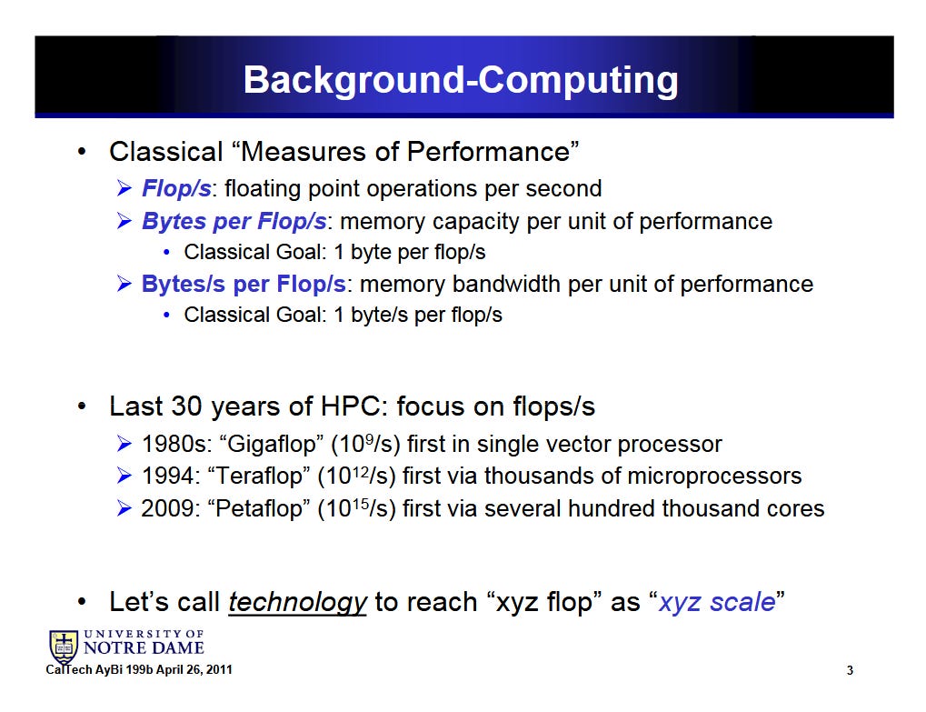
Even G80’s device memory fell well short of that goal with 1 byte/4.5 FLOPS. I prefer this framing because it adopts the viewpoint of scarcity (bytes/FLOP – getting data in and out for processing) rather than abundance (FLOPS/byte – having lots of processing power to bring to bear on data once it is in hand).
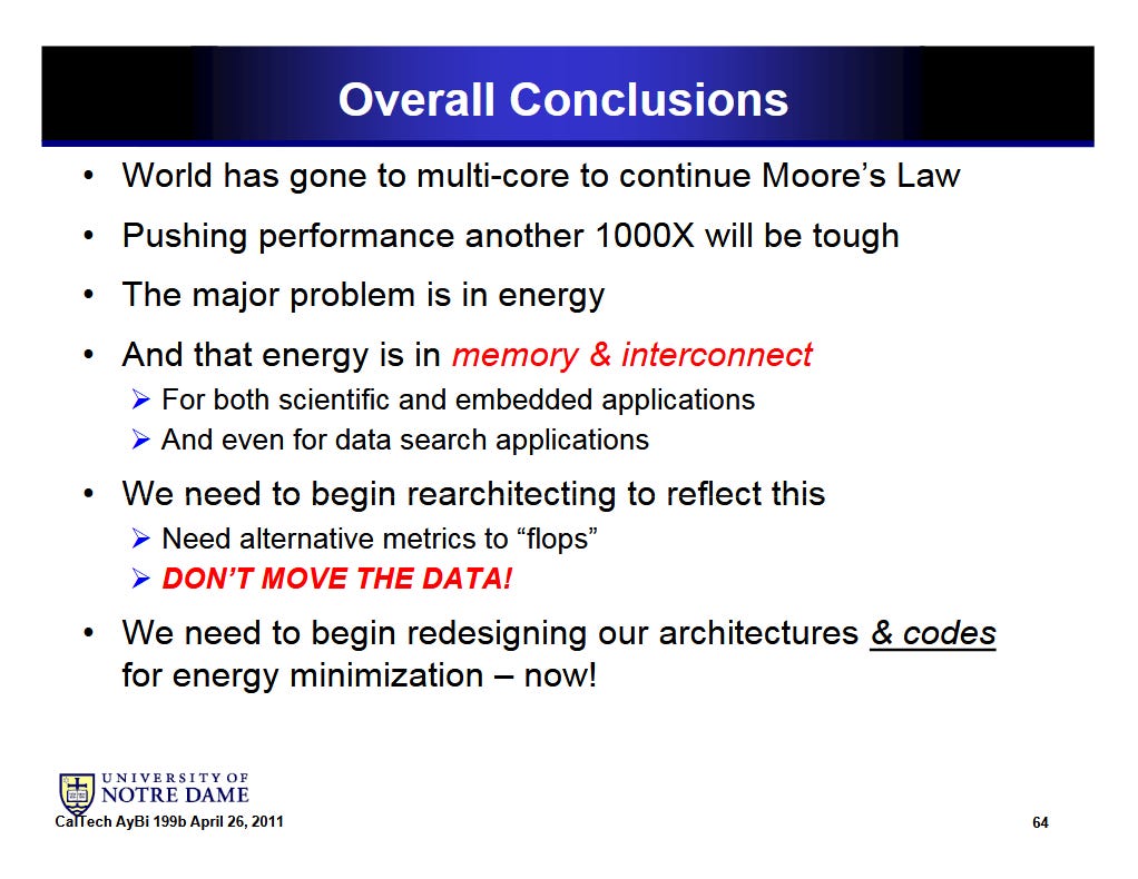
The presentation is from 2011, but still very relevant: after reviewing Moore’s Law and the rise and fall of Dennard scaling, and the preeminent importance of power dissipation in modern computing, the concluding slide reads in part:
World has gone to multi-core to continue Moore’s Law
Pushing performance another 1000X will be tough
The major problem is in energy
And that energy is in memory & interconnect
We need to begin rearchitecting to reflect this …
DON’T MOVE THE DATA!
“DON’T MOVE THE DATA” has been good advice to everyone who’s had the data for decades (in 1992 I wrote a Dr. Dobb’s Journal article that focused on hand-coding x87 assembly to keep intermediate results in registers)… but the advice has more currency now.
Moving The Data on CPUs
The data/compute conundrum finds expression on modern multi-core CPUs, too. Each core on a modern x86 CPU has ILP (instruction level parallelism) of 5, meaning it can detect parallelism opportunities between non-dependent instructions and execute up to 5 instructions in a single clock cycle. Latency to the L3 cache is about 50 clock cycles. So a CPU core can perform at least dozens, and possibly hundreds, of FLOPS on data in registers during the time it takes for the L3 to service a load (2 of the 5 pipelines can do 8 FLOPS per instruction via AVX). And that’s assuming the data was in cache!
As an aside, this observation helps explain why “optimized” numerical Python code is still dead slow. Python is interpreted, so has a library called Numpy that wraps vectorized implementations of operations that do things like element-wise addition or multiplication between arrays. But for the reasons explained above, it is very inefficient to do multiple passes over the data if the computation could have been fused into a single pass. The code spends all of its time moving data, and very little time processing it. (Python developers wishing to optimize such code can use Numba, which enables JIT compilation for operator fusion and other performance optimizations. —Ed.)
DON’T MOVE THE DATA!
A Gift From Heaven: Deep Learning
Which workloads, pray tell, require endless FLOPS per byte of I/O? Or turn it around and ask, which workloads still thrive when there is barely any I/O per FLOP? NVIDIA hasn’t been shy about trumpeting its solution to this problem: deep learning! Training a deep learning network entails refining floating point weights that roughly represent neurons that “learn” as they are trained on the data. As long as the weights can reside in device memory, only a modest amount of I/O is needed to keep the GPU busy. In retrospect, NVIDIA is extremely fortunate that deep learning cropped up. Without it, it’s not clear what workload could soak up all those FLOPS without the GPUs starving. (2025 update: At the end of 2017, NVIDIA’s market capitalization was some $117B. It is now $4.2T, 35x higher.. so to say NVIDIA is “extremely fortunate that deep learning cropped up” turned out to be the understatement of the millenium! —Ed.) The importance of machine learning as a workload helps explain why GV100 contains purpose-built hardware for machine learning, in the form of TensorCores. But that hardware actually exacerbates the GPU starvation problem, by increasing FLOPS without increasing bandwidth.
NVIDIA probably isn’t comfortable betting the farm on a single workload – especially one where their main customers are enterprises that can invest in their own machine learning hardware and that is attracting VC money for application-specific hardware. How do you hedge? How can NVIDIA relieve the bottleneck? Unless some workload materializes that is as compute-intensive (per byte of I/O) as machine learning, NVIDIA must seek out ways to address their GPUs’ I/O bottleneck. (And certainly they did, by purchasing Mellanox for their Infiniband controllers and driving continued investments into their existing NVLink and GPUDirect technologies. —Ed.)
I/O: NVIDIA’s Strategic Landscape
The problem confronted by NVIDIA is that they are hindered by some business and legal challenges. According to the terms of their 2011 settlement with Intel, 1) They do not have a license to Intel’s industry-leading cache coherency protocol technology, and 2) they do not have a license to build x86 CPUs, or even x86 emulators. (How times have changed! The details we know about the Intel/NVIDIA deal appear to be squarely aimed at granting NVIDIA access to x86 processors and Intel’s cache coherency protocol. NVIDIA can leverage the learnings from their own Grace Hopper superchip, preceded by the partnership with IBM to bring coherent access to GPU memory to servers with IBM’s POWER architecture. I don’t know about Jensen, but for NVIDIA’s sake, I was pining for access to QPI back in the late aughts! —Ed.)
NVIDIA has done what they can with the hand they were dealt – they built GPUDirect to enable fellow citizens of the bus (typically Infiniband controllers [and, since, they have added mass storage such as NVMe —Ed.]) to access GPU memory without CPU intervention; they built NVLINK, a proprietary cache coherency protocol. They have licensed NVLINK to IBM for the POWER architecture and signaled a willingness to license it to ARM licensees. The problem is that POWER and ARM64 are inferior to Intel’s x86, whose high-end CPU performance is unmatched and whose “uncore” enables fast, cache coherent access across sockets. NVIDIA itself, though an ARM licensee, has announced that they will not be building a server-class ARM chip. (In April 2021, they reversed this decision and announced Grace. NVIDIA also tried and failed to buy ARM, a $40B purchase that was announced in September 2020 and abandoned in February 2022 amidst regulatory headwinds. In a quirk of coincidence, NVIDIA paid a $1.25B penalty to Softbank after terminating the agreement, an amount reminiscent of the $1.5B paid to NVIDIA by Intel for the private antitrust settlement. —Ed.)
I’m not sure why NVIDIA announced they would not be building their own ARM to drive their GPUs, because that seems like an obvious way for them to own their destiny. It may be that NVIDIA concluded that ARM64 cores simply will never deliver enough performance to drive their GPUs. That’s too bad, because there is a lot of low-hanging fruit in NVIDIA’s driver stack. If they made the software more efficient, it could either run faster on the same hardware or run at the same speed on lesser hardware – like ARM64 cores.
Not being able to coordinate with Intel on the cache coherency protocol has cost NVIDIA big-time in at least one area: peer-to-peer GPU traffic. Intel could, but chooses not to, service peer-to-peer traffic between NVIDIA GPUs at high performance (Intel and NVIDIA give different stories as to the reason, and these conversations happen indirectly because the two companies do not seem to have diplomatic relations). As things stand, if you have a dual-CPU server (such as NVIDIA’s own DGX-1) with cache coherency links between the CPUs, any peer-to-peer GPU traffic must be carefully routed past the CPUs, taking care not to cross the cache coherency link. If Intel could license QPI to Altera, they could license it to NVIDIA. Failing to do so is a matter of choice and a by-product of the two companies’ respective positions in the business and legal landscapes.
As things stand, NVIDIA is dependent on Intel to ship great CPUs (in 2025, of course, AMD has since eaten Intel’s lunch! -Ed.) with good bus integration, and peer-to-peer-capable GPU servers have to be designed to steer traffic around the QPI link. The announcement that NVIDIA would not build ARM64 SOCs was done in 2014, so now that the competitive landscape has evolved (and though I can remember when Intel’s market capitalization was 12x NVIDIA’s, it is now only about 1.7x), it would not surprise me if NVIDIA revisited that decision. (Of course, NVIDIA did enter the server-class ARM business with Grace so my crystal ball was working that day. But if you’d told me that in 2025, NVDA would be worth $4.5T and INTC $185B, I am not sure I would have believed you. —Ed.)
One Path Forward: SoCs
One partial solution to the interconnect problem is to build a System on a Chip (SoC): put the CPU and GPU on the same die. (In 2025, packaging technology has advanced to the point where hardware designers build multi-chip implementations of such architectures, such as AMD’s MI300A or NVIDIA’s GB10. —Ed.) Intel and AMD have been building x86 SOCs for many years; it is Intel’s solution to the value PC market, and AMD has behaved like their life depended on it since 2006, when they acquired GPU vendor ATI. NVIDIA’s Tegra GPUs are all ARM SoCs. The biggest downside of SoCs is that the ratio of CPU/GPU performance is fixed years before the hardware becomes available, causing workloads to suffer if they are more CPU- or GPU-intensive than the SoC was designed to address. (This downside risk of SOC design is mitigated by chiplets, since they are separately fabricated and can even target different semiconductor nodes. —Ed.) And if the device doesn’t have enough performance, scaling performance across multiple chips may be more difficult because GPUs require such high bandwidth. A conspicuous success story for big SoCs has been in the gaming console market, where the target workload is better-understood and, in any case, game developers will code against whatever hardware is in the console.
So I suspect that as workloads continue to tap out the FLOPS and balance out the bandwidth/FLOPS, big SoCs will start to make more sense. In sizing the CPU/GPU ratio, hardware designers can create a device with the biggest possible GPU that doesn’t starve with the available bandwidth.
SoCs are just a stopgap, though. As the laws of physics continue to lower the boom, the importance of system design will continue to increase, as Kogge pointed out in his 2011 presentation. The fundamental problem of the speed of light isn’t going away… ever.
(The DGX Spark [né DIGITS] device announced at GTC 2025, of course, is a system-in-package with ARM cores and a Blackwell GPU. As far as packaging goes, NVIDIA has been late to the chiplet party, possibly due to lingering trauma from the bump crack fiasco of the 2000s; but they are on the way. —Ed.)